AVR I/O Pins
Get ready kids, this one’s a doozy. Think you have what it takes to stay awake through this diatribe? Tell you what; if you fall asleep I’ll keep it a secret. Promise.
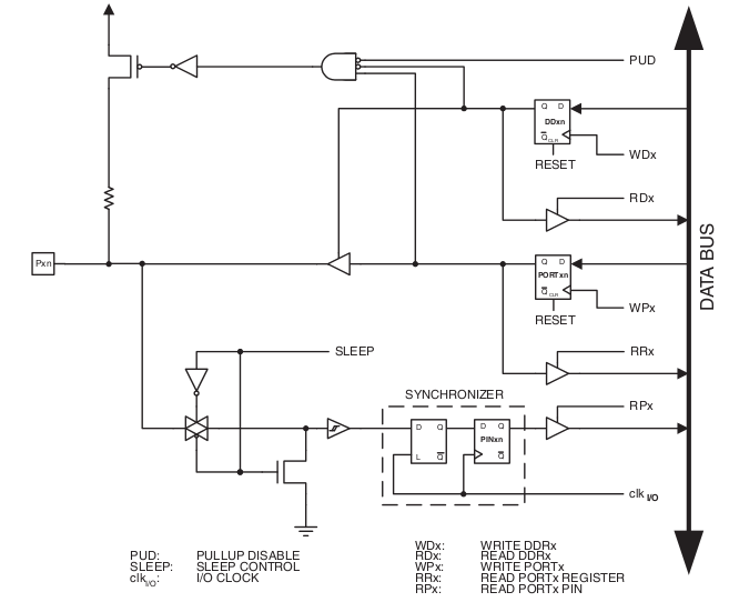
Ever wonder how the I/O pins on your AVR device work? Of course not. No one would willingly subject themselves to this schematic:
I’m here to change that. I’ll make a deal with you: stick through this, and you’ll never wonder how to drive another circuit with your AVR again.
The Magic Bus
The logic begins on the right side with two flip-flops tied to the data bus and to what they refer to as “WDx” (writes of DDRx) and “WPx” (writes of PORTx). These are going to latch the state of the data bus on writes to these registers. The diagram doesn’t make it clear, but what it means by “DATA BUS” is really the state of DDRx, PORTx, and PINx. So the top buffer latches the value of DDRx and the bottom latches PORTx. Not complicated yet!
The tri-state area
Let’s go on to the output of the PORTx flop. This continues to a tri-state buffer enabled by the output of the DDRx flop. When the enable is high the buffer is essentially a short, but when the enable is low it’s an open circuit. So in this case, when DDRx = 1 the value of PORTx will get pushed out onto the pin. When DDRx = 0 the value of PORTx has no effect (except on the pull-up logic, which we’ll get to in a second).
What we just went through covers 90% of most programs you’ll write. If you want to use the I/O port for output you do something like:
    DDRA = 0xff;
    PORTA = 0x00;
Writing DDRA will latch the value of 1, enabling the tri-state buffer. The subsequent write to PORTA will latch the value of 0, which will make its way through the buffer out to the output pin PINA.
Pull-up a chair and stay a spell
The next interesting part is the pull-up logic along the top. On the far left is a PMOS transistor connected to Vdd on one side and a resistor on the other. When this transistor is an open circuit the pull-up logic has no effect on the output pin, and it will either be left open or driven by PORTx (depending on DDRx). On the other hand, if the transistor is enabled then the resister will become the only thing between the output pin and Vdd. What does this mean? Well, the output pin can be in two different states:
-
Pxn = Vdd: There is no voltage drop across the resistor and so it drives no current to the pin.
-
Pxn = 0V: There is a voltage drop of Vdd over the resistor, and so it drives Vdd/R amps to the output pin.
When is this useful? Imagine that you’re driving an LED. You don’t want to drive the LED by just hooking one end to Vdd and one end to ground because of the low resistance of the LED: you’ll drive way too much current through it and destroy it. If, however, you use the pull-up circuit, then you’ll only drive Vdd/R amps through it - a much safer level - and you don’t need to use any external circuit to do it.
So we now now when we would want to use a pull-up circuit. Let’s now see how this pull-up logic gets activated. There’s a three-input NAND gate (well, an AND tied to an inverter) with the following inputs: not PUD, not DDRx, and PORTx. Say what now? One step at a time now:
-
not PUD (pull-up disable): an inverted disable signal. When PUD is low, the NAND input will be high, which will allow the pull-up logic set with PORTx. When PUD is high, the NAND input will be low, which will disable the pull-up transistor.
-
not DDRx: if DDRx is set the pull-up logic is disabled. When low the pull-up logic can be controlled by PORTx.
-
PORTx: directly controls the pull-up transistor. If it’s 0 the pull-up logic will be disabled, and if 1 the transistor can be set.
So, everyone say it with me: when the stars align and you meet the following conditions:
^PUD & ^DDRx & PORTxThe pull-up transistor will be enabled and the pull-up resistor will be shorted to Vdd. Whatever is attached to the output pin will be treated to Vdd/R amps.
Button it up!
There’s all that mumbo-jumbo at the bottom that deals with synchronizing and latching the correct input values, but I think we got through the most important parts here. How does it all tie together? I’ll sum it up:
-
There’s a flip-flop that latches the value of PORTx and only drives the output pin when DDRx is asserted, and is floating otherwise.
-
The pull-up logic is enabled when PUD = 0, DDRx = 0, and PORTx = 1.
Hopefully you now have the knowledge you need to interface with any sort of circuit on the output pin. I’ll be using this to figure out how to talk to my untalkative ADB mouse.