Apple A9M0331 Schematic
I spent some time this morning with a multimeter capturing what I could of the Apple A9M0331 mouse schematic. These mice were manufactured sometime in the mid-80’s while Apple was still pushing Apple Desktop Bus in its product line (one of the ICs inside has a copyright symbol dated 1986). Though I’m thinking I may have fried this particular one, it was a useful exercise and will help debug my ongoing communication issues in ADBUSB.
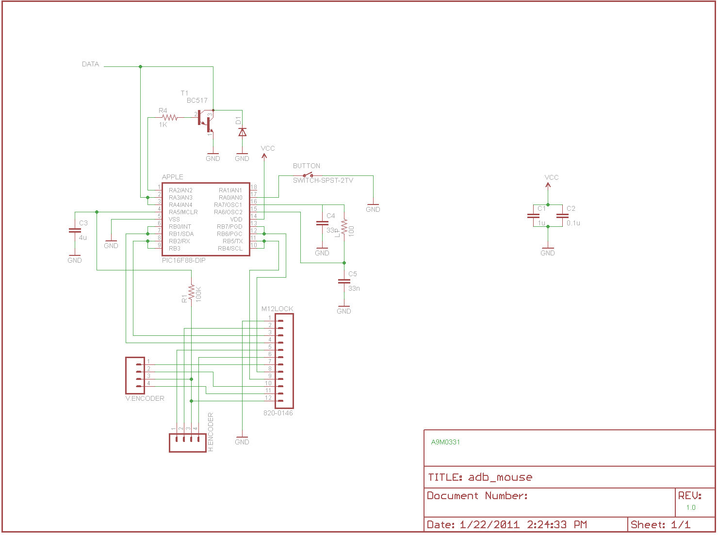
The first thing to notice is the two capacitors between Vcc and ground on the far right. This is good practice to reduce voltage spikes and dissipate any noise on the power line. Any high frequency noise components will pass straight through C1 and C2, leaving the DC signal intact to power the rest of the electronics. Both Vdd and GND are directly tied to the ADB connector. The data line is protected by a zener diode to ground. This will keep the voltage regulated at a constant value.
I was most interested in the data line, which is at the top, but let’s go from the bottom up of the schematic. There are only a few main components: the main PIC, an encoder board, two encoders to track the mouse ball, and a switch for the mouse button.
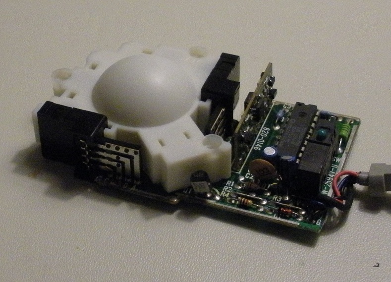
The two encoders are connected to the encoder board. In the photo above it’s the small perpendicular board in the middle with the surface-mount IC. My guess is that this translates the pulses from the two encoders to simple up/down and left/right signals for the main microcontroller. I’m also not sure how it’s powered - I couldn’t find an explicit Vcc connection so it must draw its power from the I/O pins on the PIC. Interestingly the board designer chose to duplicate all of the connections to the PIC pins. Pin 8 of the encoder board, for example, is connected to both pins 12 and 13 on the PIC. Why? Any PIC die-hards out there know?
The PIC is the brains of this mouse. Pin 4 might power the encoder board or accept input from it - I don’t know which - but it has another low-pass filter between them, making me guess it’s a power line. Pin 5 (Vss) is grounded out. Pins 6-13 (which make up port B) are all connected to the encoder board. Pins 15 and 16 look like they make up an RC oscillator circuit to clock the PIC. Pin 17, connected to the mouse button switch, is also a mystery to me. It looks like a normally-open switch that shorts to ground when the button is pressed. Now, I’m no guru, but I’m pretty sure that a floating circuit is kind of useless. Maybe it’s magic.
The logic on the top where the data line comes in is what I was looking forward to. It’s not terribly complicated, so let’s dive right in. The first connection we’ll look at is pins 2 & 3 of the PIC: tied directly to the data line on the ADB connector. We always treat IC I/O as having infinite input resistance, so no voltage will be dropped across the pin and it’s essentially a “perfect observer”. In a protocol like ADB that supports many devices listening on the same line this is necessary to prevent the signal from being degraded. Pin 1 is next and I find it interesting how they used it to control a BJT between the data line and ground. To “talk” on the line, all the PIC does is flip pin 1: that powers the base of the transistor and shorts out the data line to ground. Neat!